Focusing on 6G communication core components, with a layout of ten years, XOI is about to mass produce, and this team is working hard to optimize the process
2024-02-08
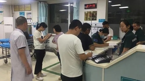
Master and apprentice Ou Xin (left) conducted in-depth research and discussion on semiconductor materials characterized and analyzed using transmission electron microscopy. Our reporter Yuan Jing photographed that as the Spring Festival approached, Ou Xin, director of the Silicon Based Materials and Integrated Devices Laboratory of the Chinese Academy of Sciences Shanghai Institute of Microsystems and Information Technology, had no time to take into account the holiday arrangements, and had been busy between the laboratory in Changning District and the engineering platform in Jiading. As an important wafer material in 5G and future 6G communication RF and optoelectronic chips, the single crystal thin film heterojunction integrated substrate developed by Ouxin's team is about to face significant applications. This Spring Festival, we will seize the time to optimize the process and improve yield. Since returning to China in 2015, Ouxin has been investing in the research of Heterogeneous Integrated Substrate Materials (XOI), and now it has finally reached industrialization. In a glass cabinet door in Ouxin's office, four or five types of XOI series wafers are displayed. "Watching them transform from 'big flower faces' to so smooth and beautiful, it feels like time is not wasted," said Ouxin. Ten years ago, in order to break through the limits of Moore's Law and aim for the development direction of future RF and optical chips, Microsystems began to lay out the development of heterojunction integrated XOI materials - a sandwich like material structure, with the top X representing any semiconductor, the middle layer being silicon dioxide, and the bottom layer being a silicon substrate. This new material is expected to replace the silicon single crystal thin film (SOI) that traditional microelectronic devices rely on, opening up new development opportunities. Especially in 5G/6G communication, artificial intelligence optoelectronic chips, and new energy power chips, heterojunction integrated XOI materials can achieve the preparation of higher frequency, higher speed, lower power consumption, and higher power devices. Nine years ago, after returning from studying abroad in Germany, Ouxin devoted herself to exploring XOI. "At first, we were not sure where XOI could be used, but just one or two years later, the arrival of the 5G era showed everyone the clear industrial needs of XOI.". Filters are one of the core components in RF front-end modules. With the widespread commercialization of 5G communication, the demand for filters in mobile terminals such as mobile phones continues to grow. For a long time, foreign countries have dominated the main market through technological and patent barriers. To bypass barriers, one must break away from the original technical framework and take a different path. Perhaps starting with new materials is a feasible path to break through the dilemma of filter technology. Ouxin led the team to start searching for answers. Shortly after Ou Xin returned to China, Huang Kai and Zhang Shibin joined his team as doctoral students, choosing heterogeneous integration XOI as their main focus. In this almost unprecedented "no man's land" exploration, the two senior brothers described this experience as "lost" and "painful". Due to the different endowments of thin film materials, it is extremely difficult to form stable wafers that resonate with the substrate material at the same frequency and can process various RF and optoelectronic devices on them. Thanks to the deep technical accumulation in the field of SOI in the laboratory, Master Ouxin and his disciples almost used the most "clumsy" trial and error methods to gradually find various performance "puzzles" of XOI materials. In the end, the research team successfully developed various heterojunction wafers that meet the requirements of RF, optoelectronic, and power device applications. Based on heterojunction wafers
Edit:Luo yu Responsible editor:Zhou shu
Source:whb.cn
Special statement: if the pictures and texts reproduced or quoted on this site infringe your legitimate rights and interests, please contact this site, and this site will correct and delete them in time. For copyright issues and website cooperation, please contact through outlook new era email:lwxsd@liaowanghn.com

 Recommended Reading Change it