Metal in the chip
2022-04-25
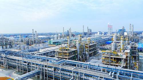
Metal materials play an important role in the evolution of chip technology. In the process of shrinking the size of advanced processes, precious metals and their alloys play a key role in realizing small linewidth, low resistivity and high adhesion. After entering the 21st century, more than 40 elements have been added to chip materials, of which about 90% are precious metals and transition metals. Precious metal is one of the promoters of advanced chip technology. Intel has recently introduced antimony and ruthenium as metal contact, which makes the capacitance smaller and breaks through the limitation of silicon. Previously, Intel took the lead in introducing cobalt material into some interconnection layers of 10nm process nodes, which improved the electron mobility by 5 ~ 10 times and tripled the path resistance. Intel is not alone in the exploration of Internet materials. Applied materials is one of the first semiconductor technology manufacturers to use Cobalt as conductor material to replace traditional copper and tungsten; Grofand also replaced tungsten with cobalt in the 7Nm process. At present, Samsung and TSMC are also actively developing new interconnection materials. It is expected that in the near future, a new generation of interconnection materials such as cobalt alloy, ruthenium and rhodium are expected to shine on the stage and build a bridge for advanced process chips. How are the roads in the "chip city" interconnected "If a chip is compared to a city, the transistor is its core area and is responsible for the operation of information. The interconnection layer is equivalent to the road of the city and is responsible for the traffic between information and the outside world." In an interview with China Electronics News, Dr. Sheng Haifeng, a senior engineer of MGG, made such a vivid analogy. Sheng Haifeng believes that under Moore's law, when the transistors in the core area become smaller and denser, the road will become narrower and denser. When the density of the core area is large to a certain extent, the transportation capacity of the road, that is, the RC delay of the interconnection layer, becomes the bottleneck of the whole chip speed improvement and power consumption reduction. In this case, the metal material of the interconnection layer needs to be upgraded to speed up the "road" of the transistor core. The continuation of Moore's law is closely related to the evolution of interconnected materials. As the technical director, Wang Chen, a researcher at Tsinghua University, has successively worked for Intel and Fanlin semiconductor, a chip equipment manufacturer, and has in-depth research on high-end chip materials and advanced chip manufacturing and architecture. Wang Chen explained to the reporter of China Electronics News that the interconnection material is actually the wire for the interconnection and transmission of electrical signals between the front-end transistor layer and the back-end external circuit layer. The enhancement of quantum effect is a major challenge for interconnected materials. Wang Chen told reporters that at present, transistors enter the sub-10nm scale in multiple geometric dimensions, and the quantum effect of materials begins to be significant. If transistors continue to shrink, they will encounter challenges in materials, processes and device structures. As the core connecting the front-end transistor layer and the outermost package planting layer, the interconnection material miniaturization of the middle end and the back end also faces the challenge of quantum effect enhancement. Copper and "Damascus process" In the 1990s, the semiconductor process entered the 0.18 micron era, and the later aluminum interconnection technology encountered a huge bottleneck. To this end, the world's major semiconductor manufacturing companies are looking for a metal that can replace aluminum. Because copper is inexpensive, conductive and easy to deposit, we all think of copper. However, because copper cannot be dry etched, the back-end interconnection problem cannot be solved. In order to find inspiration, an IBM engineer came to Damascus, known as the "garden of the world". By chance, he saw a craftsman engaged in metal inlay in a remote corner. When observing the craftsman's inlay process, engineers keep thinking of such scenes: carving is similar to etching, inlay is similar to deposition. He suddenly realized that although copper could not be etched, it could be deposited. Similar to the Damascus process, engineers can first etch the pattern film for metal wires on the dielectric layer, and then fill it with metal to realize multi-layer metal interconnection without metal layer etching. In this way, the engineer successfully solved the technical problem of copper interconnection and named the process Damascus process. The times are progressing and the line width is shrinking. In 2018, applied materials and other companies used cobalt as conductor material to replace traditional copper and tungsten wires in some fields. Referring to the intergenerational changes of aluminum, copper and cobalt wires, Sheng Haifeng told reporters that copper replaces aluminum because it has better conductivity and can reduce the resistance in RC delay. In many logic chips, copper completely replaces aluminum, that is, all interconnection layers are upgraded to copper. However, the substitution of cobalt for copper is different. Cobalt has the advantage of conductivity to copper only when the interconnection layer is very narrow, so cobalt only replaces copper in metal layer 0 (M0) and metal layer 1 (M1), and other interconnection layers will continue to use copper. From cobalt to ruthenium and rhodium Intel took the lead in introducing cobalt material into some interconnection layers of 10nm process nodes, realizing 5 ~ 10 times improvement of electron mobility and twice reduction of path resistance; Applied material is one of the first semiconductor manufacturers to use Cobalt as conductor material to replace traditional copper and tungsten; Grofand also replaced tungsten with cobalt in the 7Nm manufacturing process. How to maintain the resistivity at a low level at the scale of 20nm or even smaller is the core of the research and development of interconnection materials. Wang Chen said that although the introduction of cobalt has brought many yield and reliability problems, it is a big leap in the field of interconnection materials, breaking through the existing copper material system and improving the performance of 10nm chips as a whole. More importantly, the introduction of cobalt has made technical reserves for smaller node processes in the later stage, and it is expected that the improvement of node performance after 7Nm will be more significant. Interconnection materials are evolving towards ultra-thin, low resistivity, barrier free and low delay. At present, Samsung and TSMC are actively developing new interconnection materials. Wang Chen said that in the near future, a new generation of interconnection materials such as cobalt alloy, ruthenium and rhodium are also expected to appear. At the same time, interconnection lines without diffusion barrier layer and even embedded interconnection tracks under the transistor layer are also the direction to solve the challenge of interconnection materials. Introducing new metal materials to assist advanced manufacturing processes Precious metal materials play an important role in the evolution of chip technology. Chi Xiannian, an expert in the semiconductor industry, told China Electronics News that semiconductor chips are developing towards the trend of small volume, high speed and low power consumption. It is required that the contact resistance of the contact point is low, the thermal stability and adhesion within a wide temperature range are good, and higher requirements are also put forward for horizontal uniformity and thin diffusion layer. Therefore, in the process of shrinking the size of advanced processes, precious metals and their alloys play a key role in realizing small linewidth, low resistivity, high adhesion and low contact resistance. In the process of continuous improvement of chip process, the main challenge faced by transistors is to suppress the short channel effect. Sheng Haifeng said that at this stage, the FinFET process can be extended to 3nm at most. At 3nm and below nodes, gaafet process is the main direction. Gaafet mainly uses traditional materials, and the biggest challenge is process accuracy control. Facing this challenge, the introduction of new metal materials is more critical. Sheng Haifeng told reporters that Samsung used lanthanum doping to improve VT (threshold voltage). For the interconnection layer, the introduction of new materials includes not only the metal cobalt of the interconnection layer, but also the barrier layer between the metal of the interconnection layer and the insulating layer of the interconnection layer. The role of the barrier layer is to bond the interconnection metal and insulating layer, and improve the electron migration reliability of the interconnection layer. Tantalum and ruthenium are new elements that have been used and are being explored in the barrier layer. At present, the horn of the global 2nm chip manufacturing process war has sounded. In 2011, FinFET technology was introduced into 22nm node to replace planar transistor; New processes such as GAA and CFET are expected to be gradually introduced at about 3nm nodes. These processes will involve a lot of material problems such as doping control and strain control. Wang Chen told reporters that at the sub-1nm node, the challenges of related materials are becoming more and more prominent, and the quantum effect of materials will play a significant role. At that time, the quantum effect regulation of silicon-based materials, atomic level processing of materials and single electron fluctuation of devices will deeply challenge the existing material system and manufacturing process. It is imperative to introduce new material systems, such as layered semiconductors, new principle devices and new processing technologies. "It is reported that due to its small size, two-dimensional semiconductor materials are expected to help break through the advanced process of 2 nm." Wan Qing, a professor at the school of Electronic Science and engineering of Nanjing University, told China Electronics News. 90% of the new chip materials are metal Precious metals have excellent conductivity, stability and thermal conductivity. They are the key core materials in the semiconductor industry. After entering the 21st century, more than 40 elements have been added to chip materials, of which about 90% are precious metals and transition metal materials. It can be seen that metal materials are important in the application of chip field. Metal materials used in the field of chip manufacturing have a higher "threshold". Chi Xiannian took metals in interconnected materials as an example and told reporters that chip level metal materials should consider factors such as contact resistance and nano level adhesion. Therefore, copper, cobalt and other metals can only be used in chip manufacturing after they are made into high-purity targets or alloy targets. At present, Holly's in Germany, Honeywell International Co., Ltd. in the United States and Dongcao Co., Ltd. in Japan mainly produce chip grade copper and cobalt. Affected by the situation in Russia and Ukraine, palladium has become one of the hottest precious metals at present. Russia's Palladium production accounts for about 40% of the global total, and palladium exports account for 35%. Palladium can be used in semiconductor components such as sensors and is also one of the important raw materials in chip packaging. He Jinjiang, deputy general manager of Youyan Yijin new materials Co., Ltd., told China Electronics News that palladium and silver palladium alloys are important materials for preparing MLCC capacitors and resonators; In the packaging link of semiconductor back channel, palladium alloy and palladium plated wire are mainly used for lead bonding of electronic packaging to replace gold wire; In addition, palladium can be used as palladium alloy solder for precise connection of components. Based on the characteristics of palladium, new materials and applications are also being developed. Precious metal materials have four main applications in the field of chips. Wang Chen told the reporter of China Electronics News that the first is Internet materials. For example, from early aluminum to copper, to Al Cu alloy and tungsten, as well as the latest cobalt and ruthenium under research. The second is the metal gate material. Since Intel introduced the high dielectric metal gate transistor structure at the 45nm node in 2007, tantalum, tantalum nitride, titanium nitride, TiAlN and other material systems have been widely used, and metal silicide contact has also experienced the evolution from titanium, cobalt and nickel to metal silicide system. The third is metal barrier adhesion layer materials, such as titanium / titanium nitride, tantalum / tantalum nitride and other barrier adhesion layer materials commonly used in chip manufacturing and advanced packaging. The fourth is the metal materials for back-end packaging, including traditional lead based alloys and lead-free antimony, tin, silver and indium based alloys. In addition, the later substrate interconnection also involves a large number of precious metal materials. Among them, the nano bottom interconnection metal at the front end of the chip, metal gate material and barrier adhesion layer material are the forefront of metal material research and development. Therefore, how to maintain the characteristics of high conductivity, low electromigration, uniform crystallinity, high thermal diffusion and process integration in a small scale has become the research focus of chip metal materials and the material bottleneck of the next generation of high-performance chips. The impact of metal price rise on the chip is small
Edit:Li Ling Responsible editor:Chen Jie
Source:CHINA ELECTRONICS NEWS
Special statement: if the pictures and texts reproduced or quoted on this site infringe your legitimate rights and interests, please contact this site, and this site will correct and delete them in time. For copyright issues and website cooperation, please contact through outlook new era email:lwxsd@liaowanghn.com

 Recommended Reading Change it